
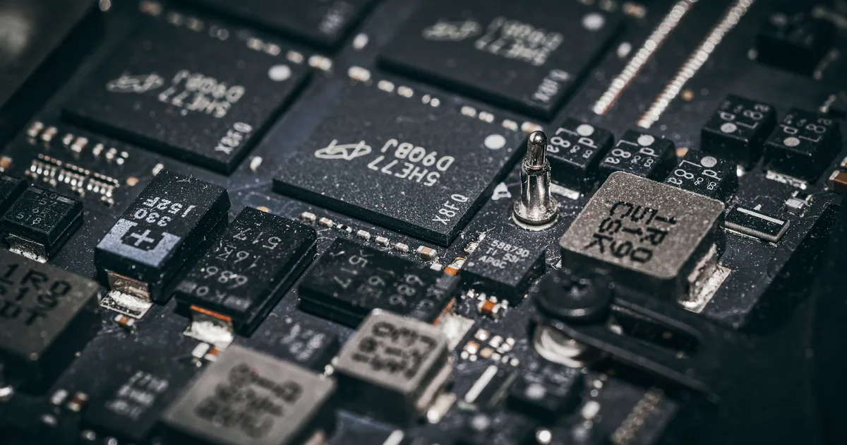
NVIDIA designs the engine for AI and builds almost none of it. Every Blackwell GPU that ends up answering your prompts was fabricated by TSMC in Taiwan, stacked with memory bought from a Korean or American supplier, mounted on a silicon interposer, bolted into a server by a Taiwanese contract manufacturer, and finally racked by a cloud provider who rents it back to you by the hour.
So when the question is who builds these engines, the honest answer is that around a dozen companies do, and NVIDIA is the one that draws them.
That distinction earns its keep. It explains why GPUs stay scarce, why the scarcity does not respond to NVIDIA hiring more engineers, and why the price of your inference bill gets set several steps upstream of anyone you could call.
What NVIDIA actually makes when it makes an AI engine
NVIDIA produces a design and the software stack that runs on it. Neither one requires a factory.
The design is the visible part. A Blackwell-architecture GPU carries 208 billion transistors, and NVIDIA's own architecture page states in the same breath that it is manufactured on a custom-built TSMC 4NP process. The foundry has never been a secret. It is printed on the marketing material.
The word engine is doing double duty here, which is probably why the question gets asked the way it does. NVIDIA ships blocks it literally calls engines inside the silicon, and the Blackwell page names three of them:
- Transformer Engine, now in its second generation, handling the low-precision arithmetic that large language models run on, down to four-bit floating point.
- Decompression Engine, which accelerates database queries.
- RAS Engine, for reliability, availability and serviceability, which predicts hardware faults before they take a training run down with them.
Then there is CUDA, the software layer that lets code written years ago run on silicon designed last year. Competitors have matched NVIDIA on raw throughput more than once. Nobody has matched fifteen years of accumulated software that already works, which is the least glamorous moat in the industry and by a distance the most effective.
What NVIDIA has never owned is a fab.
Who builds the chip, and who builds the machines that build it
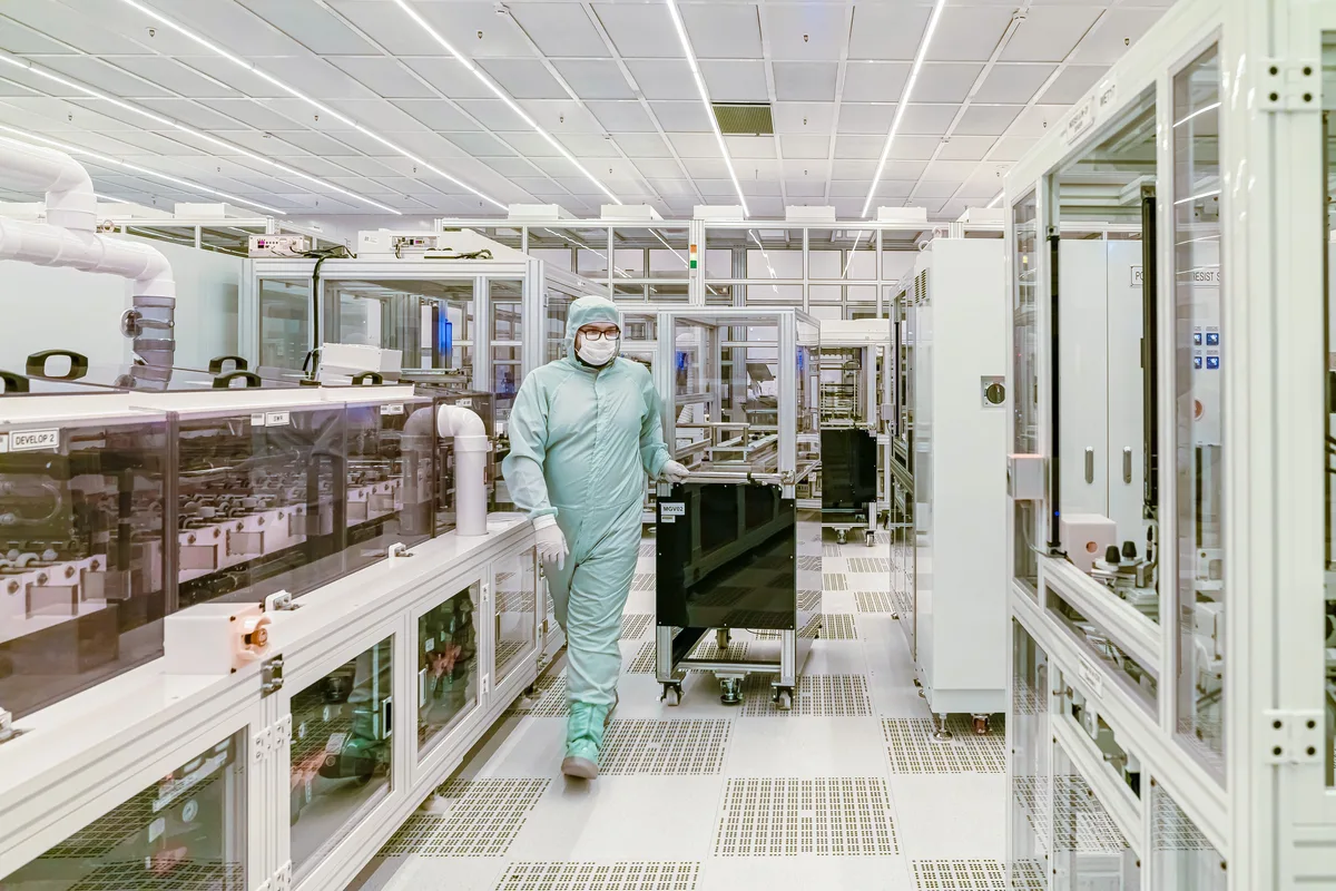
TSMC builds the chip. Taiwan Semiconductor Manufacturing Company takes the design files and turns them into patterned silicon on a process node tuned for NVIDIA's use.
A foundry, meaning a company that manufactures chips other people design, is the reason the fabless model works at all. NVIDIA and Apple among others draw processors they have no capacity to build, and TSMC converts those drawings into wafers at a scale nobody else has reached at the leading edge.
Behind TSMC sits a company most people outside the industry have never heard of. ASML, in the Netherlands, builds the lithography machines that print the transistor patterns in the first place. Its extreme ultraviolet systems work at a wavelength of 13.5 nanometres, which ASML's own product documentation describes as almost x-ray range. The light is generated by firing a CO2 laser at tin droplets up to 50,000 times per second, inside a vacuum, while the wafer stage holds position to within a quarter of a nanometre.
ASML is the only company on earth that makes them, and it describes the technology as unique to ASML. If you want one fact that explains why advanced chip supply cannot be scaled by writing a larger cheque, that is the fact.
Every leading-edge AI accelerator in the world therefore traces back through one foundry to one Dutch machine shop. Redundancy appears to have been a phase-two item.
Memory and packaging decide how many engines exist
The GPU die is only part of the product. Beside it sit stacks of high-bandwidth memory, and around both sits the packaging that wires them together.
High-bandwidth memory, or HBM, is DRAM stacked vertically and connected straight down through the silicon, which puts far more bandwidth next to the processor than a flat memory layout ever could. Those stacks come from memory manufacturers, principally SK hynix and Micron. NVIDIA buys them like anyone else buys a component.
Packaging is where the separate pieces become one part. TSMC's CoWoS platform, short for chip on wafer on substrate, mounts the logic die and the memory cubes on a shared silicon interposer that carries the connections between them. TSMC's CoWoS documentation covers interposers larger than twice the reticle size, roughly 1,700 square millimetres, because a modern accelerator no longer fits inside the area a lithography machine can expose in a single shot.
This step sets the ceiling on supply. A fab can etch more dies than there is packaging capacity to assemble them into products, and adding packaging capacity is a multi-year project. When you read that GPUs are sold out, the binding constraint usually lives here, well downstream of the transistor everyone talks about.
If you want the layer below this, where tokens and parameters turn into the memory footprint that all of the above exists to serve, LLM Systems Engineering works through it properly.
From a bare die to a rack you can plug in
A packaged GPU still cannot run anything. Several more companies have to touch it first.
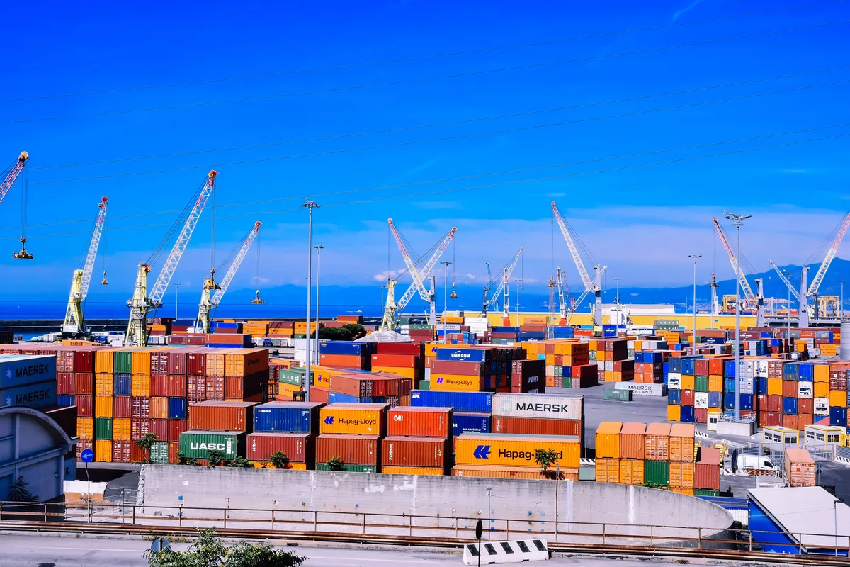
Board partners mount the package on a printed circuit board with power delivery and cooling attached. Contract manufacturers, mostly Taiwanese names such as Foxconn and Quanta, assemble those boards into servers and those servers into racks. Then the rack ships to a data centre, where the constraint stops being silicon and starts being electricity.
| Layer | Who does it | Why it bottlenecks |
|---|---|---|
| Architecture and software | NVIDIA | Design cycles run years ahead of demand |
| Lithography machines | ASML | One supplier, multi-year build times |
| Wafer fabrication | TSMC | Leading-edge node capacity is finite |
| HBM memory | SK hynix, Micron, Samsung | Stacking yields trail demand |
| Advanced packaging | TSMC and other packaging houses | Capacity takes years to add |
| Server assembly | Foxconn, Quanta, Wistron | Seldom the binding constraint |
| Deployment | Cloud providers | Power, cooling and grid connections |
Seven layers, and NVIDIA owns one of them. It happens to be the one everybody names, which is either excellent branding or the natural fate of whoever gets to put the logo on the box.
The engines that are not NVIDIA, including Apple unified memory
NVIDIA is one engine among several, and the alternatives are built by an even shorter list of companies.
Google has designed its own TPUs for a decade, and Amazon builds Trainium and Inferentia for the same reason, with AMD's Instinct line competing head on. Every one of those parts is fabricated by TSMC. Changing the logo on the accelerator changes nothing about who owns the fab.
Apple sits slightly outside the pattern. Its M-series chips use unified memory, meaning a single pool of RAM shared by the CPU and the GPU instead of two pools with a copy in between. For running a model at your desk that layout matters more than the spec sheet suggests. A large language model needs its weights resident in memory the GPU can address, and on a Mac the GPU can address nearly all of it. A machine with 64 GB of unified memory will hold models that a discrete graphics card with 24 GB will refuse.
The trade is bandwidth. Apple's memory is generous and comparatively slow next to HBM, so tokens arrive steadily instead of quickly. For a laptop running on battery that is a good deal. For serving a thousand concurrent users it is not.
What all this means if you run a local LLM
The practical version comes down to memory. For most engineers the hardware decision is a capacity question long before it is a vendor question.
To run an LLM locally the weights have to fit. A model quantised to four bits, meaning its parameters stored at reduced precision to save space, needs roughly half a gigabyte per billion parameters. A 7B model settles comfortably into 8 GB. A 70B model wants around 40 GB, which is the point where consumer hardware stops being casual about the whole idea.
Why run an LLM locally when an API call costs a fraction of a cent? Privacy is the usual answer, and it is a real one for regulated data that cannot leave a machine. Latency is the second, since a local model has no network in front of it. The third is that you stop being exposed to a supply chain seven layers deep whose capacity was decided eighteen months ago. Our piece on when to build an LLM covers the same decision from the model side, and how a large language model is actually made covers what those weights are before they reach your GPU.
Here is the rule of thumb worth keeping. When the next hardware announcement lands, the useful question is which of the seven layers gained capacity, because that is the number that reaches your bill. Speed gets announced at a keynote. Supply was decided in a packaging plant a year and a half earlier, by a company whose name was nowhere in the press release. Budgeting for the gap between the two is a large part of the AI systems engineering problem.